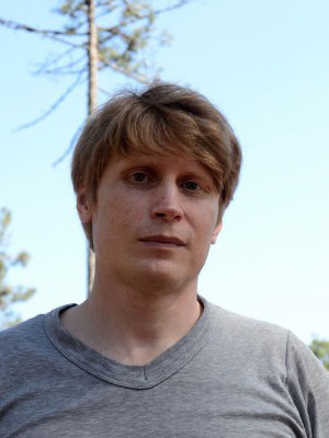
Konstantin Nikolaevich Romanyuk

Junior Researcher

short CV

ResearcherIDs:

http://www.researcherid.com/rid/J-2474-2013

http://orcid.org/0000-0002-9862-1889

http://www.scopus.com/authid/detail.url?authorId=8651668700

Degrees: 

M.Sc. and B.Sc. in Microelectronics and Semiconductor Physics Science at Novosibirsk State University, 2002.

Ph.D. (Solid State Physics), RWTH, Aachen, Germany 2009.

Work experience: 

  • present time, Post-doctoral researcher, University of Aveiro, Aveiro, Portugal.
  • 2009 – 2012, researcher at the Institute of Semiconductor Physics, Siberian Branch Academy of Science, Novosibirsk, Russia.
  • 2005 - 2009, visiting researcher at IBN of Juelich research center, Juelich, Germany.
  • 2002 – 2005,researcher at the Institute of Semiconductor Physics, Siberian Branch Academy of Science, Novosibirsk, Russia.
  • 2000 - 2002 - Research assistance MBE Laboratory of Institute of Semiconductor Physics, Siberian Branch Academy of Science, Novosibirsk, Russia.

Scientific specialization & skills

  • Li-ion batteries, Si/Ge nanostructures;
  • diffraction techniques: LEED, SPALEED;
  • scanning probe techniques: scanning tunneling microscopy (STM, STS), atomic force microscopy (PFM, ESM, SRI etc.);
  • Molecular Beam Epitaxy and Surfactant Mediated Epitaxy techniques.

main present collaborators

Russia:

Dr. A. A. Shklyaev - Novosibirsk State University (Novosibirsk)

Participating in projects

SFRH/BPD/88362/2012

"Spatially resolved study of Li-ion dynamics on the sub-10 nanometer level by Electrochemical Strain Microscope method" (2013-2014), investigator;


Development grants from the Russian Foundation for Basic Research (RFBR) ( Russia, 2001-2012), investigator.

selected publications (last 5 year)

  1. A. Nuraeva, S. Vasilev, D Vasileva, P Zelenovsky, D Chezganov, A. Esin, S. Kopyl, K. Romanyuk, V. Ya. Shur, and A. Kholkin, "Evaporation-driven Crystallization of Diphenylalanine Microtubes for Microelectronic Applications", Cryst. Growth and Des., 2016, DOI: 10.1021/acs.cgd.5b01604
  2. V. Ya. Shur, D. A. Bykov, K. N. Romanyuk, E. L. Rumyantsev, R. M. Kadushnikov, V. V. Mizgulin, E. Seyedhosseini, A. L. Kholkin, "Formation of Self-Assembled Pattern of Glycine Microcrystals, Experiment and Computer Simulation", Ferroelectrics, 2016, DOI: 10.1080/00150193.2016.1155401
  3. S. Y. Luchkin, K. Romanyuk, M. Ivanov, A. L. Kholkin, "Li transport in fresh and aged LiMn2O4 cothodes via electrochemical strain microscopy", Journal of Applied Physics, Vol. 118, 2015, p. 072016.
  4. V. V. Atuchin, V. A. Golyashov, K. A. Korolkov, A. S. Kozhukhov, V. N. Kruchinin, I. D. Loshkarev, L. D. Pokrovsky, I. P. Prosvirin, K. N. Romanyuk, O. E. Tereshchenko, "Crystal growth of Bi2Te3 and noble cleaved (0001) surface properties", Journal of Solid State Chemistry, 2015, DOI: 10.1016/j.jssc.2015.07.031
  5. G. Da Cunha Rodrigues, P. Zelenovskiy, K. Romanyuk, S. Luchkin, Y. Kopelevich, A. Kholkin, "Strong piezoelectricity in single-layer graphene deposited on SiO2 grating substrates", Nature Communications, Vol. 6, 2015, p. 7572.
  6. K. Romanyuk, S. Y. Luchkin, M. Ivanov, A. Kalinin, A. L. Kholkin, "Single and Multi- Frequency Detection of Surface Displacement via Scanning Probe Microscopy", Microscopy and Microanalysis, Vol. 21, 2015, p. 154-163.
  7. A. A. Shklyaev, K. N. Romanyuk, S. S. Kosolobov, "Surface morphology of Ge Layers epitaxially grown on bare and oxidized Si(001) and Si(111) substrates", Surface Science, Vol. 625, 2014, p. 50-56.
  8. S.A. Teys, K. N. Romanyuk, B. Z. Olshanetsky, "Structure of initial Ge nanoclusters at the edges of Si(111) steps with the front in the <-1-1 2> direction", Journal of Crystal Growth, Vol. 404, 2014, p. 39-43.
  9. K. N. Romanyuk, A. A. Shklyaev, B. Z. Olshanetsky, "Structure and stability of Ge clusters on Si(111) surface in the presence of Bi surfactant", Surface Science, Vol. 617, 2013, p. 68-72.
  10. V. A. Golyashov, K. A. Kokh, S. V. Makarenko, K. N. Romanyuk, I. P. Prosvirin, A. V. Kalinkin, O. E. Tereshchenko, A. S. Kozhukhov, D. V. Sheglov, S. V. Eremeev, S. D. Borisova, E. V. Chulkov, “Inertness and degradation of (0001) surface of Bi2Se3 topological insulator”, J. of Appl. Phys.,  Vol. 112,   2012, p. 113702.
  11. S. Korte, K. Romanyuk, B. Schnitzler, V. Cherepanov, B. Voigtlander, S. N. Filimonov, “Selective Adsorption of C60 on Ge/Si Nanostructures”, Physical Review Letters, Vol. 108, 2012, p. 116101.
  12. V.V. Atuchin, V.A. Golyashov, K.A. Kokh, I.V. Korolkov, A.S. Kozhukhov, V.N. Kruchinin, S.V. Makarenko, L.D. Pokrovsky, I.P. Prosvirin, K.N. Romanyuk, and O.E. Tereshchenko, “Formation of Iinert Bi2Se3(0001) Cleaved Surface”, Crystal Growth and Design, Vol. 11, 2011, p. 5507-5514.
  13. O.E. Tereshchenko, K.A. Kokh, V.V. Atuchin, K.N. Romanyuk, S.V. Makarenko, V.A. Golyashov, A.S. Kozhuhov, I.P. Prosvirin, A.A. Shklyaev, “Stability of (0001) surface of topological insulator Bi2Se3”, JETP Letters, Vol. 94, 2011, p. 500-503.
  14. A.A. Shklyaev, K.N. Romanyuk, A.V. Latyshev, and A.V. Arzhannikov, “Effect of Dislocations on the Shape of Islands during Silicon Growth on the Oxidized Si(111) Surface”, JETP Letters, Vol. 94, 2011, p. 442-445.
  15. K.N. Romanyuk, A.A. Shklyaev, B.Z. Olshanetsky, A.V. Latyshev, “Formation of Ge clusters at a Si(111)-Bi-root 3 x root 3 Surface”, JETP Letters, Vol. 93, 2011, p. 661-666.
  16. K. Romanyuk, V. Cherepanov, B. Voigtlander, “Symmetry and shape of Reconstructed Two-dimensional Islands”, Physical Review B, Vol. 83 (20), 2011, p. 205413.
  17. J. Brona, V. Cherepanov, K. Romanyuk, B. Voightlander, “Formation of pits during growth of Si/Ge nanostructures”, Surface Science, Vol. 604, 2010, p. 424-427.
  18. K. Romanyuk, J. Brona, and B. Voigtlander, “Namoscale Pit Formation at 2D Ge Layers on Si: Influence of Energy and Entropy”, Physical Review Letters, Vol. 103, 2009, p. 096101.
  19. R.A. Zhachuk, K.N. Romanyuk, S.A. Teys, B.Z. Olshanetsky, “Initial Stages of Germanium Growth on the Si(7710) Surface”, Physics of the Solid State, Vol. 51, Issue 1, Jan 2009, p. 202-207.
  20. M.V. Yakushev, D.V. Brunev, K.N. Romanyuk, et al., “Surface Morphology of a Si(310) Substrate Used for MBE of CdHgTe: I. Clean Si(310) Surface”, Journal of Surface Investigation-X-Ray Synchrotron and Neutron Techniques, Vol. 2, Issue 1, Feb 2008, p. 114-119.
  21. M.V. Yakushev, D.V. Brunev, K.N. Romanyuk, et al., “Surface Morphology of a Si(310) Substrate Used for MBE of CdHgTe: II. Si(310) Surface Annealed in As-4 Vapors”, Journal of Surface Investigation-X-Ray Synchrotron and Neutron Techniques, Vol. 2, Issue 3, Jun 2008, p. 433-439.
  22. K. Romanyuk, J. Myslivecek, V. Cherepanov, T. Sekiguchi, S. Yoshida, K. M. Itoh, B. Voigtlander,  “Optimized Ge nanowire arrays on Si by modified surfactant mediated epitaxy”
    Physical Review B, Vol. 75 (24), 2007, p. 241309.
  23. K. Romanyuk, V. Cherepanov, B. Voigtlander, “Symmetry Breaking in the Growth of Two-Dimensional Islands on Si(111)”, Physical Review Letters, Vol. 99, 2007, p. 126103.

Publications

Nanoplasmonic response of porous Au-TiO2 thin films prepared by oblique angle deposition

Rodrigues, MS; Borges, J; Proenca, M; Pedrosa, P; Martin, N; Romanyuk, K; Kholkin, AL; Vaz, F
2019, NANOTECHNOLOGY, 30, 22.
ISBN: 1361-6528

Diphenylalanine-Based Microribbons for Piezoelectric Applications via Inkjet Printing

Safaryan, S; Slabov, V; Kopyl, S; Romanyuk, K; Bdikin, I; Vasilev, S; Zelenovskiy, P; Shur, VY; Uslamin, EA; Pidko, EA; Vinogradov, AV; Kholkin, AL
2018, ACS APPLIED MATERIALS & INTERFACES, 10, 12, 10543-10551.

Kelvin force and Raman microscopies of flat SiGe structures with different compositions grown on Si(111) at high temperatures

Shklyaev, AA; Bolotov, L; Poborchii, V; Tada, T; Romanyuk, KN
2018, MATERIALS SCIENCE IN SEMICONDUCTOR PROCESSING, 83, 107-114.

Quantitative characterization of the ionic mobility and concentration in Li-battery cathodes via low frequency electrochemical strain microscopy

Alikin, DO; Romanyuk, KN; Slautin, BN; Rosato, D; Shur, VY; Kholkin, AL
2018, NANOSCALE, 10, 5, 2503-2511.

Surface potential distribution of multilayer graphene using Kelvin probe and electric-field force microscopies

Vidyasagar, R; Camargo, B; Romanyuk, K; Kholkin, AL
2017, FERROELECTRICS, 508, 1, 115-123.

Self-Assembly of Organic Ferroelectrics by Evaporative Dewetting: A Case of beta-Glycine

Seyedhosseini, E; Romanyuk, K; Vasileva, D; Vasilev, S; Nuraeva, A; Zelenovskiy, P; Ivanov, M; Morozovska, AN; Shur, VY; Lu, HD; Gruverman, A; Kholkin, AL
2017, ACS APPLIED MATERIALS & INTERFACES, 9, 23, 20029-20037.

Evaporation-Driven Crystallization of Diphenylalanine Microtubes for Microelectronic Applications

Nuraeva, A; Vasilev, S; Vasileva, D; Zelenovskiy, P; Chezganov, D; Esin, A; Kopyl, S; Romanyuk, K; Shur, VY; Kholkin, AL
2016, CRYSTAL GROWTH & DESIGN, 16, 3, 1472-1479.

Correspondence: Reply to 'On the nature of strong piezoelectricity in graphene on SiO2'

Rodrigues, GD; Zelenovskiy, P; Romanyuk, K; Luchkin, S; Kopelevich, Y; Kholkin, A
2016, NATURE COMMUNICATIONS, 7.

Crystal growth of Bi2Te3 and noble cleaved (0001) surface properties

Atuchin, VV; Golyashov, VA; Kokh, KA; Korolkov, IV; Kozhukhov, AS; Kruchinin, VN; Loshkarev, ID; Pokrovsky, LD; Prosvirin, IP; Romanyuk, KN; Tereshchenko, OE
2016, JOURNAL OF SOLID STATE CHEMISTRY, 236, 203-208.

Formation of self-assembled pattern of glycine microcrystals: experiment and computer simulation

Shur, VY; Bykov, DA; Romanyuk, KN; Rumyantsev, EL; Kadushnikov, RM; Mizgulin, VV; Seyedhosseini, E; Kholkin, AL
2016, FERROELECTRICS, 496, 1, 20-27.

We use cookies for marketing activities and to offer you a better experience. By clicking “Accept Cookies” you agree with our cookie policy. Read about how we use cookies by clicking "Privacy and Cookie Policy".