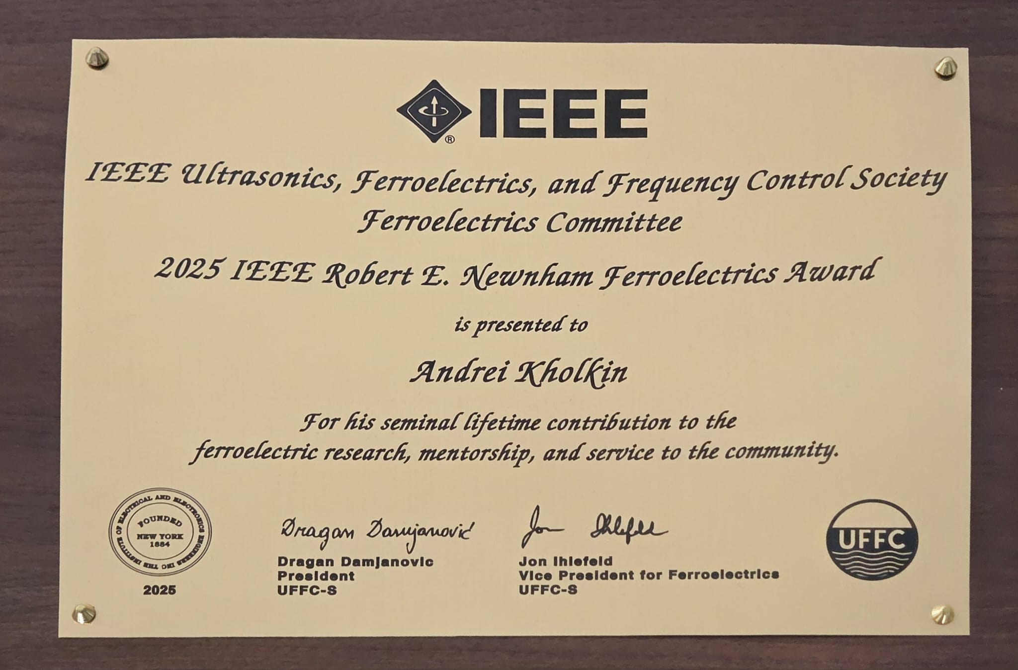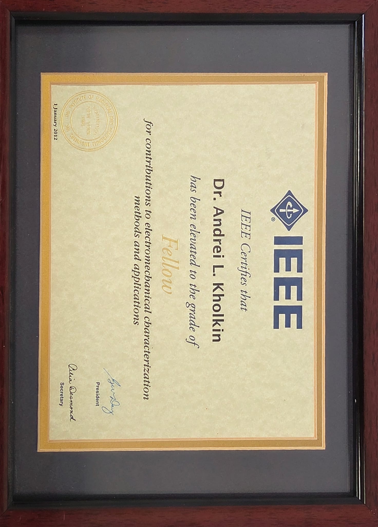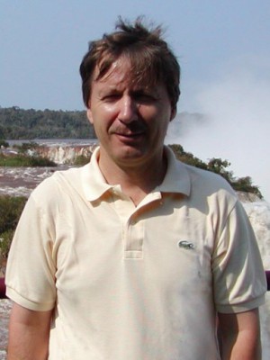
Professor Andrei L. Kholkin has played a transformative role in advancing nanoscale characterization and functional materials research at the University of Aveiro and CICECO. Through pioneering contributions in piezoresponse force microscopy, ferroelectrics, multiferroics, and bioorganic piezoelectric materials, his work has consistently bridged fundamental nanoscale science with real-world applications in energy, sensing, and healthcare. As founder of the Advanced Microscopy of Functional Materials laboratory and a leading figure within CICECO, he has contributed decisively to the development of internationally recognised research in functional materials, fostering method innovation, international collaboration, and scientific excellence.
Your scientific career spans institutions in Russia, Switzerland, the United States, Germany, and Portugal. Which experiences or environments were most formative in shaping your approach to functional materials and nanoscale characterization?
Joining CICECO when it was born in 2001 and creating the Advanced Microscopy of Functional Materials laboratory later on was indeed transformative for my career. CICECO offered a multidisciplinary environment where chemists, physicists, engineers, and biologists can work side by side and where European and national collaborations have become routine. That setting encouraged me to combine two things I care about: inventing and improving scanning probe microscopy (SPM) measurement tools, and using those tools to understand fundamental materials properties and to solve their synthesis and applications hurdles. During my overall stay in Aveiro University (1999-2024) we have advanced several local electromechanical imaging methods like Piezoresponse Force and Electrochemical Strain Microscopies (PFM and ESM, respectively) and immediately applied them to emerging materials such as lead-free piezoelectrics, ferroelectric relaxors, multiferroics, Li-ion battery materials and various biological piezoelectrics such as amino acids and peptides. My earlier periods (working in Russia, Germany, Switzerland and the US) exposed me to different cultures in terms of research and development problem framing but only in CICECO I learned how to scale those approaches into a real team work and various collaborative projects that delivered both new science and novel materials useful for industry and healthcare.
You have contributed extensively to ferroelectrics, multiferroics, piezo- and magnetoelectric materials, and advanced scanning probe microscopy techniques. How have these research directions evolved over time, and what conceptual or technical challenges defined key turning points in your career?
My scientific trajectory moved from fundamental studies of ferroelectrics and superconductors toward two tightly linked goals: reliable, quantitative nanoscale characterization, and application of those methods to diverse functional materials. The big technical turning point was learning to separate genuine material signals from artefacts produced by the SPM tip, environment or measurement setup. That led us to develop modern protocols and software for quantitative PFM and ESM measurements that could be trusted across different labs. Conceptually, the later turning point was connecting our early nanoscale observations to real device level properties—showing, for example, how domain structures in ferroelectrics influence macroscopic piezoelectric performance, or how ionic motion at the nanoscale affects energy storage or Li-ion battery cathodes. Persistent challenges remain: interpreting complex, coupled signals (electrical, mechanical, ionic), running true in situ experiments (temperature, atmosphere, bias), and bringing this knowledge into novel manufacturable materials.
Your leadership at CICECO has included coordination of European projects, organisation of international conferences, and mentoring of researchers. From your perspective, what were the critical strategies and organisational choices that helped consolidate CICECO as a leading institute in functional materials?
Three practical strategies made a difference. First, I concentrated effort on a clear technical identity—advanced scanning probe microscopy—so the lab became the “go to” place for nanoscale electromechanical, electrical and mechanical characterization. Second, I built partnerships: coordinating European projects, forming industry links, and running national consortia brought resources, diverse expertise, and real problems for the lab to solve. Third, community building—hosting conferences (including the organization of PFM meeting series or different ferroelectric symposia under the IEEE umbrella) and training students and postdocs—amplified our visibility and created a network of alumni and collaborators who spread methods and standards worldwide. Equally important was mentoring: keeping a stable core of junior researchers who could lead different subprojects and translate nanoscale methods into applications kept the group productive and resilient.
With a research portfolio spanning multiferroics, biomaterials, energy harvesting systems, and graphene-based materials, how do you balance fundamental investigation with potential societal and industrial applications?
I used a two-track model. One track pursues curiosity driven questions—how does a ferroelectric domain switch at the nanoscale, or how does ion transport couple to mechanical strain in an ionic conductor? The second track partners with industry, biologists or engineers to build demonstrators: energy harvesters, bioactive fibers, scaffolds, or point of care diagnostic components. The link between tracks is method development: when we create robust measurement tools, those tools serve both fundamental discovery and applied optimization. For example, by quantifying electromechanical response in lead free ceramics we contributed to materials selection for greener sensors; by characterizing biopolymer scaffolds we helped tune properties relevant to tissue integration and biological effects. This dual approach preserves scientific freedom while creating clear routes to societal benefit.
Over decades of international collaboration and teaching, how have you seen the field of materials science evolve, particularly regarding interdisciplinarity, instrumentation, and sustainability?
Materials science shifted from single discipline to an inherently interdisciplinary endeavor. Problems in energy, healthcare or electronics now require chemists, physicists, biologists and engineers working together. Instrumentation also evolved: single purpose instruments gave way to multimodal, in situ platforms—scanning probes combined with optical, electrical and environmental control so we can watch how materials operate under realistic conditions. Sustainability moved from niche to mainstream: researchers now routinely ask about lifecycle, toxicity and recyclability when they start designing new materials. At CICECO our projects followed these trends—collaborative teams, multimodal characterization, and an emphasis on renewable organic crystals, lead free materials and energy efficiency.
Considering your extensive publication record, citations, and patents, how do you define scientific impact, and which three achievements do you consider most transformative in advancing knowledge or influencing the field?
I define impacts as (i) creating methods or ideas that other researchers routinely use afterwards, (ii) training early-stage researchers who go on to lead their own work, and (iii) producing demonstrable breakthroughs that society can later adopt. From my work in Portugal, three achievements stand out:
First, developing and standardizing quantitative PFM/ESM methods that made nanoscale electromechanical and ionic imaging more reliable and broadly adoptable. These research protocols helped other groups interpret nanoscale signals correctly and compare experimental results across different labs. Second, establishing the Advanced Microscopy of Functional Materials laboratory at CICECO and turning it into a multidisciplinary facility that supports synthesis, modeling and device testing—amplifying the CICECO’s overall research output. Third, organizing community venues (PFM workshop series, international symposia on ferroelectrics and polar dielectrics, exchange programs like Erasmus Mundus or Research and Innovation Staff Exchange) that structured our field, accelerated method dissemination, and connected academics with industrial partners.
What advice would you offer to early-career researchers aiming to develop a career in functional materials, piezoelectric systems, and nanoscale characterisation, particularly regarding research independence, collaboration, and long-term vision?
Focus on technical excellence and clarity. Become deeply competent in one or two core methods so people seek your expertise, but keep broad collaborations to apply those skills to new problems. Start with small, independent projects that you can lead and publish, then expand into larger collaborative grants. Communicate methods clearly—others can reuse what you build, and that spreads your influence. Finally, maintain a long-range view: pick research directions that address important societal needs (energy, health, sustainability, manufacturability) and be patient—impact often takes years and multiple collaborations.
Measuring impact
Looking back at your career, which three scientific milestones do you consider transformative, either in terms of advancing knowledge or shaping research directions?
I can indicate three major scientific and organizational milestones:
- Building the Advanced Microscopy of Functional Materials laboratory within CICECO which became a sustained institutional strength and world leader in nanoscale electromechanical and other functional materials characterisation.
- Producing robust, quantitative PFM/ESM methodologies and demonstrating their application across various classes of materials: ferroelectric oxides, polymers, bioorganic materials, ionic conductors, battery materials, all of these helped to move nanoscale electromechanics from merely qualitative imaging to quantitative science and technology.
- Discovery of high piezoelectricity and ferroelectricity in a number of novel materials and structures ranging from hydroxyapatite to novel graphene-based nanostructures and bioorganic materials (e.g. amino acids, self-organized peptides, etc).