Abstract
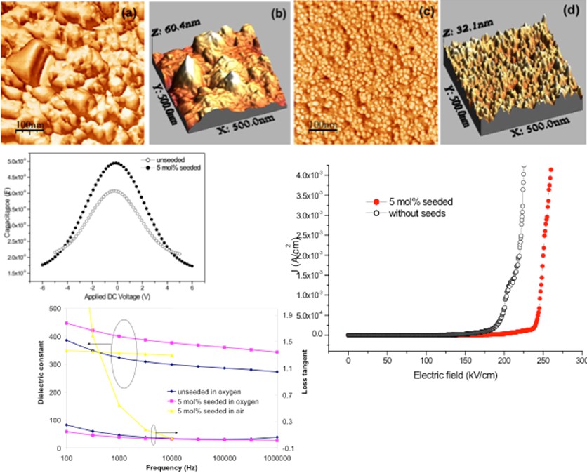
The present invention relates to a new process for obtaining thin films of dielectric, piezoelectric and ferroelectric materials at low temperatures, crystalline, dense and with optimized electrical properties, in particular barium and strontium titanate, BST, at low temperatures, 600 °C. Conventional sol gel solutions are mixed with perovskite ceramic particles with same/different solutions composition and nanometric dimensions. The principle involved is heterogeneous nucleation and energy activation reduction required for the formation of the crystalline phase, reducing films crystallization temperature, allowing compatibility with silicon technology and with low-cost substrates (steel, glass, non-noble metals), opening these films applications range and the possibility for new devices development. The relevance of the invention relates also to the possible application to many other electroceramic systems, anticipating the extension of existing applications and manufacture of new electronic devices.
Innovative aspects & main advantages
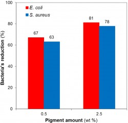
Development of a method of manufacturing dielectric piezoelectric and ferroelectric thin films by a modified sol gel method which allows the fabrication of crystalline and monophasic thin films with thicknesses of less than 800 nanometers and at low temperatures (below 600 °C, for BST thin films), dense, crack-free, with optimum dielectric properties (especially tunability of the dielectric permittivity for BST thin films) in which a wide range of non-refractory substrates can be used. And manufacture of thin films of single phase barium and strontium titanate (BST) with optimal dielectric properties, including tunability of the dielectric permittivity.
Applications
For applications in microelectronics, particularly in microelectronic mechanical systems (MEMS - microelectronic mechanical systems) and tunable devices such as filters (tunable filters), networks (tunable matching network) and oscillators (high frequency tuning range voltage controlled oscillators (VCO).
Inventors
Vilarinho, Paula; Wu, Aiying; Gao, JieOur Inventors

Aiying Wu
Researcher
Paula Maria Lousada Silveirinha Vilarinho
Vice DirectorApplicant
Universidade de AveiroGroups Involved
Related Patents
Expanded clay containing sludge generated in the paper pulp production process
Batista, João; Ferreira, Victor; Correia, António
Modified cellulose pulps, a method of high pressure processing for preparing same and uses thereof
Evtyugin, Dmitry; Saraiva, Jorge; Santos, Andreia
Method of forming an oxide thin film
Pinna, Nicola; Rauwel, Erwan
Lignocellulosic composites and phase transition materials for thermo insulation and energy storage
Coutinho, João ; Neto, Carlos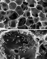
Preparation method of polymer-based composite porous structures for tissue engineering application
Fernandes, Maria; Vilarinho, Paula; Silva, Ana; Barroca, Natália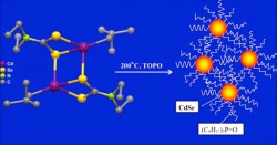
Process for preparing a nanocrystalline material
O’Brien, Paul; Trindade, Tito