Abstract
A thin oxide film is formed by atomic layer deposition (ALD) onto a substrate by exposing the substrate to a first precursor comprising a metal alkoxide or amide or heteroleptic derivatives thereof and subsequently exposing the substrate to a second precursor comprising an ALD compatible carboxylic acid or carboxyl acid derivative compound. The sequential exposure to the first and second precursors may be repeated until a sufficient film thickness of a metal oxide has been deposited on the substrate. This process allows growth of an oxide thin film or nanostructure, on any suitable substrate.
It permits formation of a high-k dielectric oxide thin film on the substrate with similar dielectric properties to a much thinner SiO2 film.
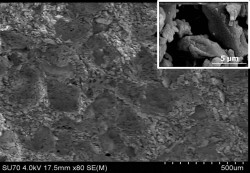
Furthermore, the films grown can exhibit very good structural and physical properties. The process also provides high self-control of thin film growth with high reproducibility and reliability. In particular, the films can be synthesized with excellent similarity even on uneven surfaces and present a very smooth surface finish with very low roughness.
Innovative aspects & main advantages
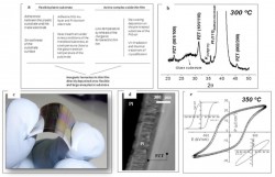
We are developing a new process to synthesize oxide thin films. The synthesis of oxide thin films requires usually high temperature (> 400°C), high vacuum, and expensive equipment. We propose a novel method based on the Atomic Layer Deposition technique (ALD) which reduces cost by allowing us to deposit at low temperature (100 to 300°C) and by using inexpensive precursors. We obtain uniform thin films with small roughness and good electrical properties.
The advantages of this method over existing methods are:
No growth of the interfacial SiO2 layer;
No contamination of impurities (i.e. the reaction is complete);
It is economical advantageous (inexpensive precursors and deposition technique allowing large scale processing);
The thickness of the film can be precisely controlled (i.e. at Angstrom level);
The technique is easy to set up and to utilize.
Applications
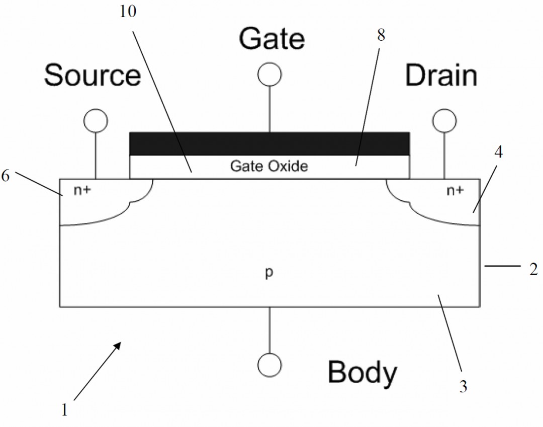
Gate oxide in Complementary metal–oxide–semiconductor (CMOS) devices; Dielectric in dynamic random-access memory (DRAM) capacitors; Deposition of metal oxides onto substrates sensitive to oxidation.


